Smooth sailing for electrons in graphene

two panels in heat-map style. both panels have circles in the middle. The panel on the left has more yellow and red to the left of the circle and a bright yellow ring around the circle; the right panel has a less sharp transition of colors from left to right and no bright ring around the circles.

Physicists at the University of Wisconsin–Madison directly measured, for the first time at nanometer resolution, the fluid-like flow of electrons in graphene. The results, which will appear in the journal Science on Feb. 17, have applications in developing new, low-resistance materials, where electrical transport would be more efficient.

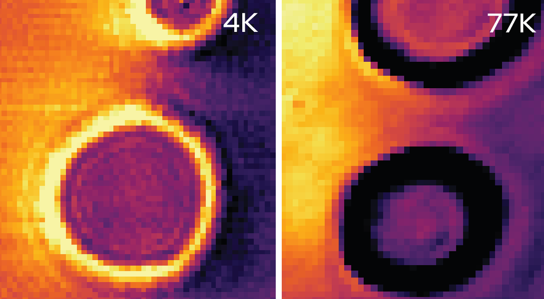
Graphene, an atom-thick sheet of carbon arranged in a honeycomb pattern, is an especially pure electrical conductor, making it an ideal material to study electron flow with very low resistance. Here, researchers intentionally added impurities at known distances and found that electron flow changes from gas-like to fluid-like as temperatures rise.

“All conductive materials contain impurities and imperfections that block electron flow, which causes resistance. Historically, people have taken a low-resolution approach to identifying where resistance comes from,” says Zach Krebs, a physics graduate student at UW–Madison and co-lead author of the study. “In this study, we image how charge flows around an impurity and actually see how that impurity blocks current and causes resistance, which is something that hasn’t been done before to distinguish gas-like and fluid-like electron flow.”

Read the full story

Flexible, easy-to-scale nanoribbons move graphene toward use in tech applications

From radio to television to the internet, telecommunications transmissions are simply information carried on light waves and converted to electrical signals.

black and white scanning electron micrograph of the nanoribbons that looks like finger prints or a 'zen garden'
University of Wisconsin–Madison researchers produced the smallest ribbons of graphene yet created, at about 12 nanometers in width, in efforts to use the all-carbon, ultra-thin and adaptable material to improve internet and other kinds of telecommunications performance. The structures, which act like tiny antennas that interact with light, are too small to see with the naked eye. IMAGE COURTESY OF STUDY AUTHORS.

Silicon-based fiber optics are currently the best structures for high-speed, long distance transmissions, but graphene — an all-carbon, ultra-thin and adaptable material — could improve performance even more.

In a study published April 16 in ACS Photonics, University of Wisconsin–Madison researchers fabricated graphene into the smallest ribbon structures to date using a method that makes scaling-up simple. In tests with these tiny ribbons, the scientists discovered they were closing in on the properties they needed to move graphene toward usefulness in telecommunications equipment.

“Previous research suggested that to be viable for telecommunication technologies, graphene would need to be structured prohibitively small over large areas, (which is) a fabrication nightmare,” says Joel Siegel, a UW–Madison graduate student in physics professor Victor Brar’s group and co-lead author of the study. “In our study, we created a scalable fabrication technique to make the smallest graphene ribbon structures yet and found that with modest further reductions in ribbon width, we can start getting to telecommunications range.”

For the full story, please visit: https://news.wisc.edu/flexible-easy-to-scale-nanoribbons-move-graphene-toward-use-in-tech-applications/

Q-NEXT collaboration awarded National Quantum Initiative funding

The University of Wisconsin–Madison solidified its standing as a leader in the field of quantum information science when the U.S. Department of Energy (DOE) and the White House announced the Q-NEXT collaboration as a funded Quantum Information Science Research Center through the National Quantum Initiative Act. The five-year, $115 million collaboration was one of five Centers announced today.

Q-NEXT, a next-generation quantum science and engineering collaboration led by the DOE’s Argonne National Laboratory, brings together nearly 100 world-class researchers from three national laboratories, 10 universities including UW–Madison, and 10 leading U.S. technology companies to develop the science and technology to control and distribute quantum information.

“The main goals for Q-NEXT are first to deliver quantum interconnects — to find ways to quantum mechanically connect distant objects,” says Mark Eriksson, the John Bardeen Professor of Physics at UW–Madison and a Q-NEXT thrust lead. “And next, to establish a national resource to both develop and provide pristine materials for quantum science and technology.”

Read the full story

New method measures temperature within 3D objects

University of Wisconsin–Madison engineers have made it possible to remotely determine the temperature beneath the surface of certain materials using a new technique they call depth thermography. The method may be useful in applications where traditional temperature probes won’t work, like monitoring semiconductor performance or next-generation nuclear reactors.

Many temperature sensors measure thermal radiation, most of which is in the infrared spectrum, coming off the surface of an object. The hotter the object, the more radiation it emits, which is the basis for gadgets like thermal imaging cameras.

Depth thermography, however, goes beyond the surface and works with a certain class of materials that are partially transparent to infrared radiation.

“We can measure the spectrum of thermal radiation emitted from the object and use a sophisticated algorithm to infer the temperature not just on the surface, but also underneath the surface, tens to hundreds of microns in,” says Mikhail Kats, a UW–Madison professor of electrical and computer engineering. “We’re able to do that precisely and accurately, at least in some instances.”

Read the full story here.

four infrared images of the fused silica window used
An infrared image of the fused silica window used to test the depth thermography concept. For the project, the team heated the silica, a type of glass, and analyzed it using a spectrometer. They then measured temperature readings from various depths of the sample. IMAGE COURTESY OF MIKHAIL KATS