Chicago Quantum Exchange Profile: Jennifer Choy

WQI’s Jennifer Choy was recently featured as part of a series of profiles of scientists and engineers from across the Chicago Quantum Exchange member institutions. This post was originally published by CQE


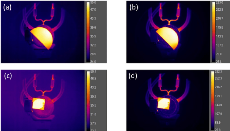
Jennifer Choy is an assistant professor of engineering physics at the University of Wisconsin–Madison who studies quantum sensing and nanophotonics. She aspires to be a great mentor to undergraduate and graduate students and encourages students to study quantum science, even if they don’t plan to go into the field.

Tell us about what you’re working on now.

We are developing miniaturized and mobile quantum sensors and engineering quantum platforms to improve their sensing performance. We are interested in two material platforms in particular: neutral atoms and solid-state color centers. Our group is applying techniques in nanoscale optics and integrated photonics to exert precise control over atom-photon interactions and miniaturize atomic sensors. We are currently developing chip-scale, near-infrared polarization optics for alkali vapor magnetometers, which could enable compact, sensitive magnetic-field-imaging devices.

How does UW–Madison help advance your work?

UW-Madison has a strong research community in quantum computing and sensing platforms and is supported by groups across many science and engineering departments. It has been very inspiring and exciting to establish relationships and collaborations with top-notch quantum researchers at UW-Madison and in the Midwest under the Wisconsin Quantum Institute and the Chicago Quantum Exchange.

How did you become interested in quantum research?

As a freshman in the Nuclear Science and Engineering department at MIT, I joined David Cory’s group, working on using liquid-state nuclear magnetic resonance as a testbed for quantum computing. I think how someone gravitates toward a field depends greatly on formative experiences and environments. I had no prior knowledge in quantum physics, but graduate students in the group were very supportive and David always graciously answered questions and offered advice, even long after I graduated. I aspire to being able to foster a similar mentoring approach and attitude.

What does the future hold for quantum technology? 

The use of quantum science in sensors and sensing brings a set of tools that can promise greater sensitivity and accuracy than conventional technologies, some of which are already in use. However, to make the next leap to other practical applications outside of the lab, a combination of fundamental science research and engineering will be needed to realize functional and robust sensor systems. Broader applications would include quantum accelerometers, gyroscopes, and clocks that can provide accurate navigation solutions without the need for GPS.

Quantum technology has a workforce shortage. What would you say to a young person who is interested in studying quantum information science?

I think part of the excitement of working in the field of quantum information science is that it offers interesting research directions in almost every science and engineering discipline. Developing quantum technologies requires partnership among academia, national labs, and industry. With several federally funded quantum initiatives, job opportunities will likely open up in all these sectors.

As someone who worked in industry (as a scientist at Draper Laboratory), what I really appreciated about my training in quantum research is that I was able to apply my skills to other unrelated fields, which were just as interesting and fulfilling. Therefore, I think a quantum workforce will generate well-rounded talents that will also benefit other industries.

Q-NEXT collaboration awarded National Quantum Initiative funding

The University of Wisconsin–Madison solidified its standing as a leader in the field of quantum information science when the U.S. Department of Energy (DOE) and the White House announced the Q-NEXT collaboration as a funded Quantum Information Science Research Center through the National Quantum Initiative Act. The five-year, $115 million collaboration was one of five Centers announced today.

Q-NEXT, a next-generation quantum science and engineering collaboration led by the DOE’s Argonne National Laboratory, brings together nearly 100 world-class researchers from three national laboratories, 10 universities including UW–Madison, and 10 leading U.S. technology companies to develop the science and technology to control and distribute quantum information.

“The main goals for Q-NEXT are first to deliver quantum interconnects — to find ways to quantum mechanically connect distant objects,” says Mark Eriksson, the John Bardeen Professor of Physics at UW–Madison and a Q-NEXT thrust lead. “And next, to establish a national resource to both develop and provide pristine materials for quantum science and technology.”

Read the full story

UW–Madison named member of new $25 million Midwest quantum science institute

As joint members of a Midwest quantum science collaboration, the University of Wisconsin–Madison, the University of Illinois at Urbana–Champaign and the University of Chicago have been named partners in a National Science Foundation Quantum Leap Challenge Institute, NSF announced Tuesday.

The five-year, $25 million NSF Quantum Leap Challenge Institute for Hybrid Quantum Architectures and Networks (HQAN) was one of three in this first round of NSF Quantum Leap funding and helps establish the region as a major hub of quantum science. HQAN’s principal investigator, Brian DeMarco, is a professor of physics at UIUC. UW–Madison professor of physics Mark Saffman and University of Chicago engineering professor Hannes Bernien are co-principal investigators.

“HQAN is very much a regional institute that will allow us to accelerate in directions in which we’ve already been headed and to start new collaborative projects between departments at UW–Madison as well as between us, the University of Illinois, and the University of Chicago.” says Saffman, who is also director of the Wisconsin Quantum Institute. “These flagship institutes are being established as part of the National Quantum Initiative Act that was funded by Congress, and it is a recognition of the strength of quantum information research at UW–Madison that we are among the first.”

Read the full story

cartoon showing a quantum hardware network
In a hybrid quantum network, hardware for storing and processing quantum information is linked together. This design could be beneficial for applications that rely on distributed quantum computing resources. | Credit: E. Edwards, IQUIST

New method measures temperature within 3D objects

University of Wisconsin–Madison engineers have made it possible to remotely determine the temperature beneath the surface of certain materials using a new technique they call depth thermography. The method may be useful in applications where traditional temperature probes won’t work, like monitoring semiconductor performance or next-generation nuclear reactors.

Many temperature sensors measure thermal radiation, most of which is in the infrared spectrum, coming off the surface of an object. The hotter the object, the more radiation it emits, which is the basis for gadgets like thermal imaging cameras.

Depth thermography, however, goes beyond the surface and works with a certain class of materials that are partially transparent to infrared radiation.

“We can measure the spectrum of thermal radiation emitted from the object and use a sophisticated algorithm to infer the temperature not just on the surface, but also underneath the surface, tens to hundreds of microns in,” says Mikhail Kats, a UW–Madison professor of electrical and computer engineering. “We’re able to do that precisely and accurately, at least in some instances.”

Read the full story here.

four infrared images of the fused silica window used
An infrared image of the fused silica window used to test the depth thermography concept. For the project, the team heated the silica, a type of glass, and analyzed it using a spectrometer. They then measured temperature readings from various depths of the sample. IMAGE COURTESY OF MIKHAIL KATS

Chicago Quantum Summit to gather international experts

abstract graphic of atoms

Top experts in quantum technology from around the globe — including experts from the Wisconsin Quantum Institute — will gather at the University of Chicago on Oct. 25 to discuss the future of quantum information science and strategies to build a quantum workforce.

The second annual Chicago Quantum Summit, hosted by the Chicago Quantum Exchange, will engage scientific and government leaders and the industries that will drive the applications of emerging quantum information science.

Read the full story here. 

WQI scientists earn grant to improve materials for quantum sensing, computing

Researchers at the Wisconsin Quantum Institute (WQI) have been awarded a US Department of Energy grant to study the noise that hampers advances in quantum systems, including quantum computers.

The three-year, $4 million funding will allow the researchers to apply emerging tools to identify new materials and fabrication methods that can improve the performance of these systems.

“All of physics is quantum on some level, and quantum systems let you understand how physics works when you get to the cleanest, smallest, most isolated systems,” says Shimon Kolkowitz, assistant professor of physics at the University of Wisconsin–Madison and lead investigator of the grant. “We think that quantum computing, and quantum technologies more generally, are a really promising area of technological development and research.”

Quantum systems — which make use of single atoms or electrons and the quantum mechanical properties that govern them — have the potential to push boundaries in such areas as computing, precision sensing, and secure communications.

Quantum computers, for example, allow scientists to simulate quantum mechanics in ways that classical computers cannot. But, the computing power of quantum computers has not yet exceeded classical ones.

a grayscale image of a scanning electron micrograph of one of the double quantum dot qubits
A scanning electron microscope image of a gate-defined double quantum dot qubit fabricated by the Eriksson group.

A limiting factor in quantum computing power is the number of qubits, or quantum bits, that can be strung together. Like bits in a classic computer, the more qubits in a quantum computer, the more the computing power. And the limiting factor in how many qubits can be connected with each other while remaining in the fragile quantum states required to perform a computation — called “coherence”  in quantum lingo — is their resistance to external environmental factors, or “noise” that may cause them to “decohere.”

However, researchers have found that the materials used to make the qubits themselves generate a lot of this noise.

“People for quite a while have seen this noise, treated it as a fact of nature, and tried to design around it. But no one really knows what it is or how to get rid of it,” Kolkowitz says. “Even more fundamentally than just understanding or reducing this noise, we think that if you can reduce or ultimately eliminate this noise, it actually opens up the design space for the kinds of qubits you can build, and that will make it much easier to wire qubits together.”

With the DOE funding, Kolkowitz, along with colleagues at WQI and the Livermore National Laboratory, seeks to first identify the nature of the noise and how specific materials contribute to it, and then to develop ways to reduce it.

small white dots, representing single atom defects, are visible in a dark purplish background that is from a diamond
Atom-size quantum defects in a diamond, imaged using a confocal microscope in the Kolkowitz lab.

Work in Kolkowitz’s group, as well as that of Victor Brar, assistant professor of physics and co-investigator on the grant, has led to the development of quantum sensors that allow the researchers to characterize things like magnetic fields at the nanometer scale, or to see how single atoms are arranged in various materials. Part of the DOE funding will be used to continue improving these sensors.

Kolkowitz and Brar then want to use their sensors to identify the noise affecting qubits designed by UW quantum computing researchers Mark Eriksson and Robert McDermott.

“And then we can work in a feedback loop, where, for example, Robert McDermott makes samples and characterizes their performance, then we study the noise limiting that performance with these quantum and nanoscale probes to figure out what’s happening on the microscopic scale,” Kolkowitz says. “Then, we give that information to our theory collaborators here and at Livermore who build models and simulations based on what we’ve measured. And then Robert can use what we’ve learned to design and make new samples to see if we’ve improved on these issues.”

scanning tunneling micrograph showing graphene with a single atomic defect as a white dot in the center.
An image taken with a scanning tunneling microscope of a single atomic defect in graphene

Trying to identify sources of this noise is nothing new, but what Kolkowitz finds most promising about the work funded through this grant is the development and application of new sensing technologies.

“These emerging tools that use quantum states and quantum systems themselves should give us access to the origins and behavior of noise in quantum platforms on scales that haven’t been accessible before,” Kolkowitz says.

Other WQI members who are co-investigators on the grant include Jennifer Choy, Laura Faoro, Mark Friesen, and Alex Levchenko.

Not so defective, after all: Demystifying advanced quantum materials

Sometimes, flaws are what makes a thing special.

That’s the case for a type of material called optical quantum emitters, which send out light in an exceptionally precise manner, one photon at a time, often due to tiny imperfections in a crystal’s structure.

The ability to emit light one photon at a time could allow optical quantum emitters to become the backbones of ultrafast computers, super high-resolution sensors and uncrackable long-range secure communication technologies.

Recently, buzz has been building about a newly discovered variety of quantum emitters consisting of two-dimensional materials (think flat sheets only as thick as a single molecule, similar to graphene). But there’s a hitch: No one truly understands the exact natures of the tiny flaws, called defects, that cause these two-di materials to become optical quantum emitters. And that’s been a major obstacle in obtaining these potentially useful materials.

This story continues on the College of Engineering’s site.